|
LabGuy's World: NTSC Sync Generator Printed Circuit Board Project [HOME] [ELECTRONICS PROJECTS] 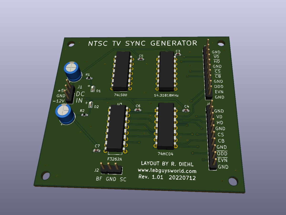
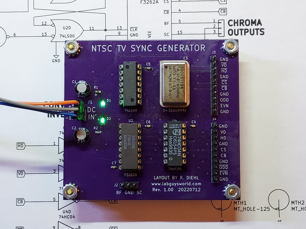
A complete television sync generator for the experimenter When a person chooses to experiment with classic analog television circuits, a video sync pulse generator is an excellent tool to have. The sync generator is the heart of virtually all video sources. Such as: video cameras, video scanners, test signal generators, frame buffers, etc. This NTSC SYNC GENERATOR BOARD generates a complete set of timing pulses conforming to the American NTSC standard. The board can be used for testing experimental circuits or it can be directly incorporated into a permanent project if the space is available. The board measures 3 inches by 2.75 inches and is 7/8" high on its standoffs. (76.2mm x 69.85mm x 22.2mm) 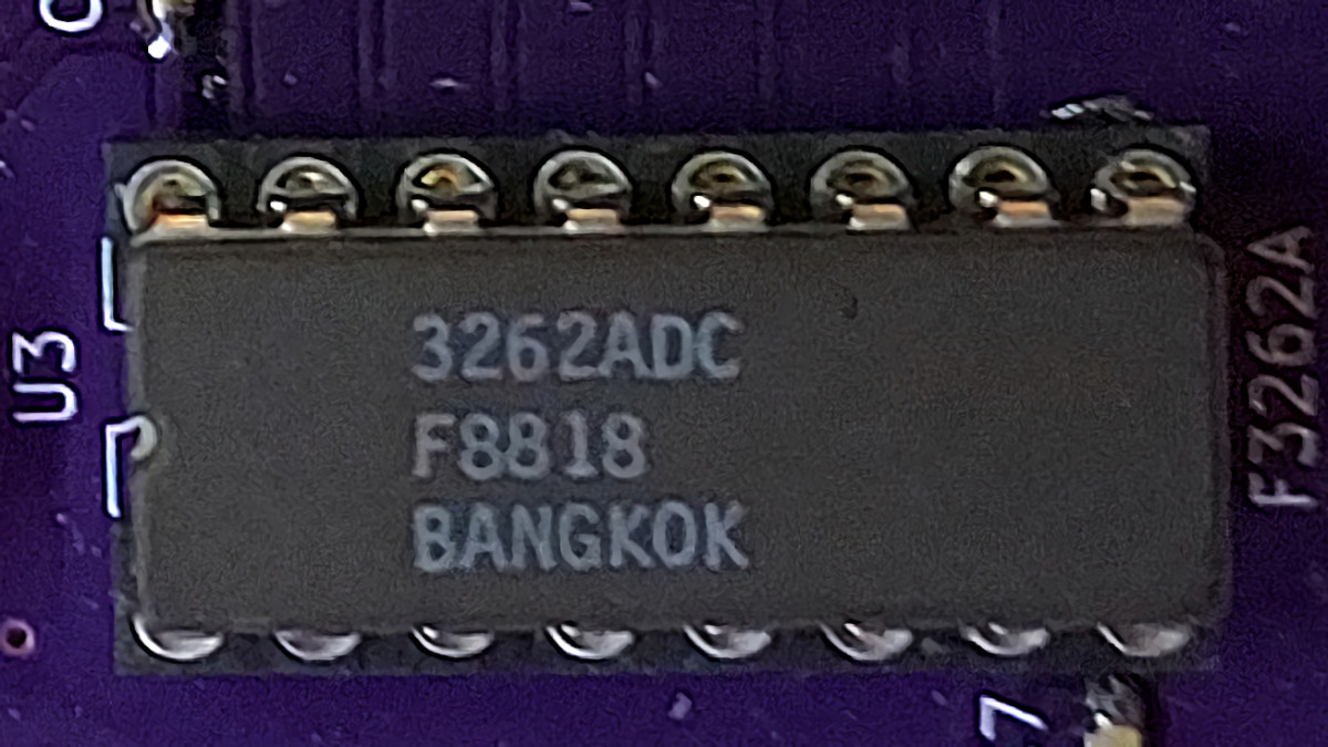
The project is based on my favorite TV sync generator chip, the [Fairchild F3262ADC]. This chip was designed in the late 1970s or very early 1980s. The part we are using on this board comes in a ceramic 16 pin classic DIP package. The remaining three chips are 14 pin DIPs. The board uses all single row pin headers for I/O. There are two 3 pin headers and two 10 pin headers. It is the user's choice whether to install male of female SIP connectors. Top of the board or bottom. J1 is the input for power. J2 is access to the F3262ADC's NTSC color signals. J3 are the remaining sync generator outputs in their true states. J4 has the same signals as J3, but each signal is inverted. This is extremely convenient when bread boarding. Plenty of ground pins are provided as well. The remainder of the components consist of two electroytic capacitors, five ceramic SMT (0603) capacitors, two SMT (0603) resistors and two SMT (0603) LEDs. 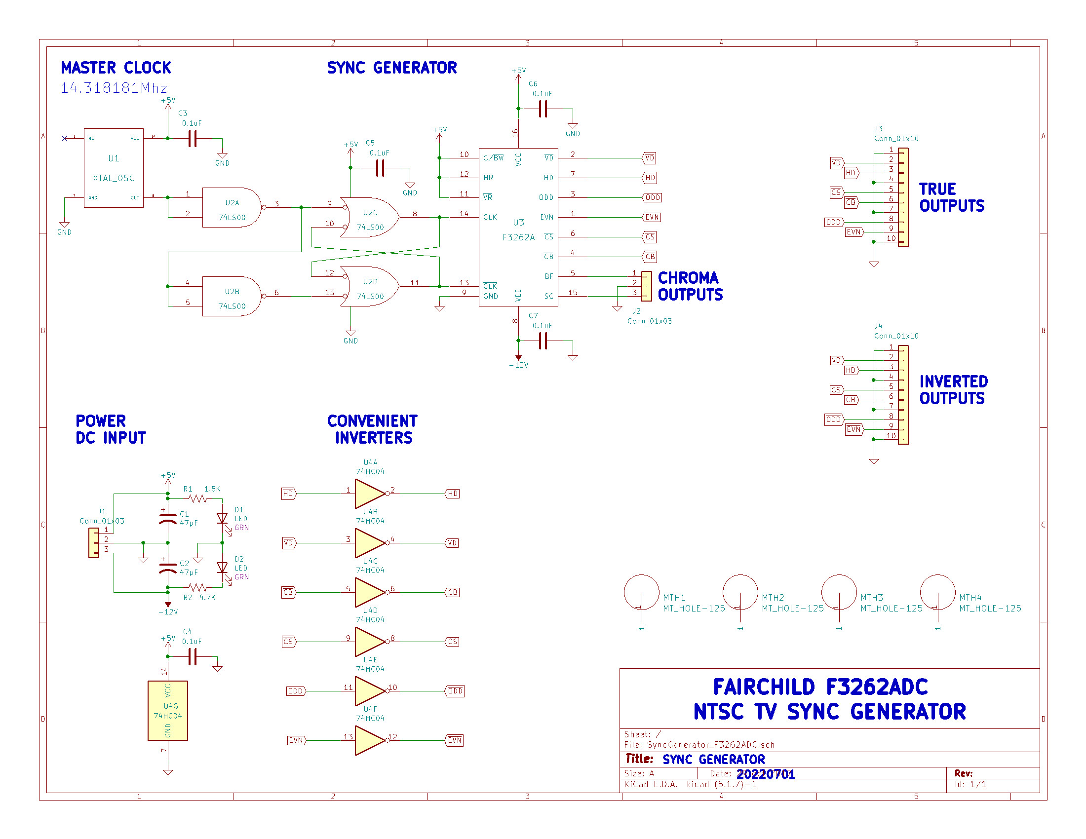
Schematic diagram and theory of operation The Fairchild F3262ADC is fully complient with the RS-170EIA specified output signals. All of the timing diagrams are in the PDF datasheet located near the bottom of this page. Master clock (MCLK) is provided by a 14.31818MHz crystal oscillator, U1. MCLK is then converted from a single phase to two phase clock by U2, a 74LS00 quad two input nand gate. The two phase clock is delivered to U3, F3262ADC, which generates all of the other signals. U4, a CMOS TTL hex inveter, gives us the complimentary forms of six of the pulses. (HD, VD, CB, CS, ODD and EVN) for easier bread boarding. The board runs on +5V at 55.2mA and -12V at 26.4mA, for a total power consumption of just under 0.6 watts. A pair of convenient, emerald green, power LEDs are provided to warn the experimenter that power is applied. NTSC Sync Generator Output Signal Definitions: The precise timing details are fully defined on pages 4 and 5 of the [Fairchild F3262A Datasheet]. Read more about the derivation of the NTSC standard here: [Wikipedia - NTSC] Horizontal Drive: This pulse is for driving the horizontal scan circuit in CRTs, and camera tubes, and or can be used to indicate start of a new line in digital systems. This pulse is active low. It is low for 10.5µS and high for approximately 54µS. Vertical Drive: This pulse is for driving the vertical scan circuit in cathode ray, and or camera tubes, and can be used to indicate start of a new field (every 262.5 lines) in digital systems. This pulse is also active low. It is low for 9.5 TV lines and High for 253 TV lines. Odd / Even Field: These two pulses are active high and each one occurs in alternate fields. The field pulses are high for 4.5 TV lines and low for 520.5 TV lines. The start of each field pulse corresponds to the rising edge of vertical drive pulse for that field. Composite sync: Is composed from four separate signals. These are: Horizontal Sync, Vertical Sync, Equalizing Pulses and Serration Pulses. Horizontal sync is a low going pulse that is 4.89µS wide and continuously repeating at the TV line rate. The vertical sync puls is also an active low pulse that is 3 TV lines wide (approx' 191µS) and repeats at the field rate of 59.94Hz (15,734.266 Hz / one field or 262.5 TV lines). Equalizing pulses and serration pulses operate at twice the horizontal frequency (2H), are narrower than H sync pulses, and are inserted into the first 9 TV lines of the vertical blanking interval. The function of these 2H rate pulses is archaic by today's standards. But, in its time, these pules helped to prevent unwanted DC shifts in AC coupled, vacuum tube based, vertical sync detecting circuits (and is also beyond the scope of this text). One final comment on THIS signal vs the others. The composite output from the F3262ADC is bandwidth limited so that it may be added directly to a video signal without using a bandwidth limiting circuit first. The other pulses have rise and fall times that exceed the bandwidth of NTSC as delivered by the F3262ADC. Composite Blanking: Is composed of horizontal blanking pulses and vertical blanking pulses. Composite blanking is an active low signal. When active, the electron beam in the CRT or camera tube is turned off for the scan retrace period(s) by this signal. Horizontal blanking pulses are low for 10.76µS and high for 52.74µS. Vertical blanking is low for 21 TV lines (1.33mS) and high for 241.5 TV lines (15.35mS). These two signals are logically "ORed" together to form the complete composite blanking signal. Burst Flag: Or "Burst Gate" is the signal which tells the downstream color encoder when to insert the color burst into the composite video signal. This is the reference subcarrier pulse that synchronizes the color local oscillator to the 3.58MHz in the composite video signal. Burst is effectively, another sync pulse dedicated to the chroma decoder (QUAM Demodulator) in receiving equipment. The color burst is placed on the back porch of the horizontal sync interval which is encompassed by the horizontal blanking pulse. Burst occurs just after the horizontal sync pulse and persists for 8 to 10 cycles of SC. Sub Carrier: More properly called "Color Subcarrier". This is the continuous carrier wave for the quadruture modulation scheme used to encode the color difference signals and add them to the baseband composite video. It is a steady 3.579545MHz derived by dividing the 14.31818MHz clock by 4. This is the only non-digital output, ignoring composite sync. It's output level is only 0.5V, high impedance and must be AC coupled and amplified before it can be used. A 3.58MHz bandpass filter in this path does no harm as well. Please NOTE. In my years of experience with this chip, I have never personally used the chroma signals (BF and SC). Yes. An NTSC encoder is on my video projects bucket list. Sync Generator Waveforms (Actual O'Scope Screen Shots) 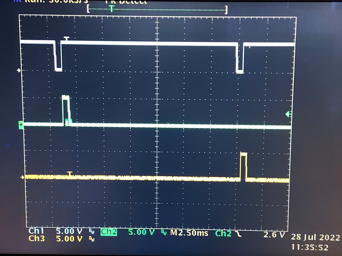
Vertical Drive (VD), Odd Field (ODD) and Even Field (EVN). VD occurs in every field. Odd and Even show up in alternating fields. Remember that a Frame is made of two interlaced Fields standard definition television. 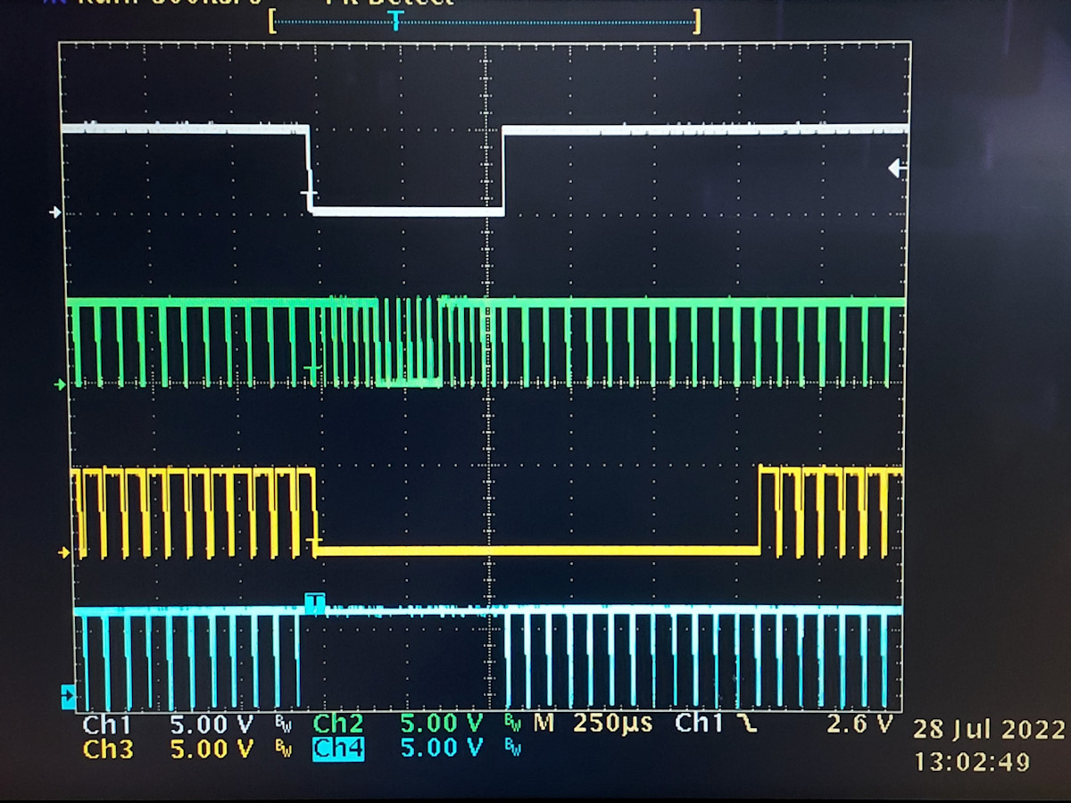
Vertical Drive (VD), Composite Sync (CS), Composite Blanking (CB) and Burst Gate (BG). VD encompasses the first 9 TV lines of the vertical blanking interval and is intended for the vertical deflection circuit. Composite sync is composed of Vertical sync, Horizontal Sync, Equalization pulses and Serration pulses and is attached to the composite signal to pass these pulses to down stream equipment. Composite blanking is used to enable / disable the scanning beam in camera tubes or as a signal or sync gate in video procesing circuitry. Burst Gate occurs on most TV lines in the Horizontal Blanking interval. As shown, Burst Gate is suppressed for much, but not all, of the Vertical Blanking interval. 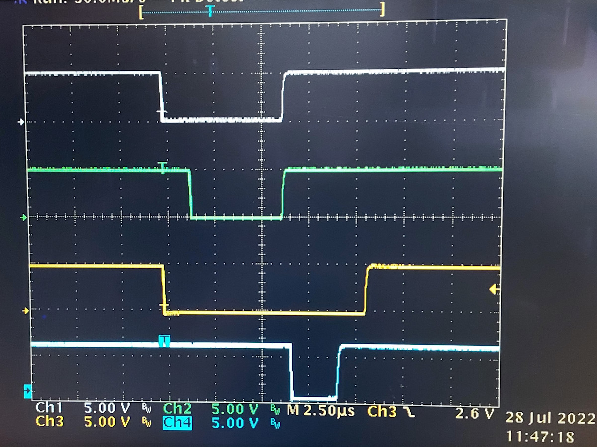
Horizontal Drive (HD), Composite Sync (CS), Composite Blanking (CB) and Burst Gate (BG). Horizontal Drive occurs on every TV line and is intended for the scan circuit. Composite sync and Composite Blanking is defined in the previous paragraph. Burst Gate occurs on most TV lines in the Horizontal Blanking interval. Burst Gate occurs on the back porch of Horizontal Blanking and indicates when to insert an 8 to 10 cycle sample the Color Subcarrier (SC) at the correct reference phase and amplitude. 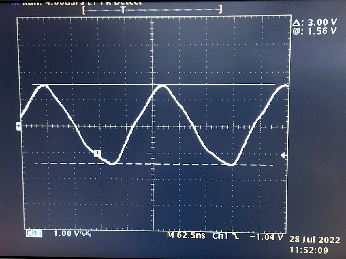
Color Subcarrier (SC). This signal is the only non digital output from the F3262ADC chip. It is about 3Vpp, sitting on about a +2V DC offset above ground. Clearly, the raw waveform is not a very clean sine wave. This signal is typically AC coupled to a gain stage and then passed through a 3.58MHz band pass filter to clean it up and remove unwanted harmonics before use. 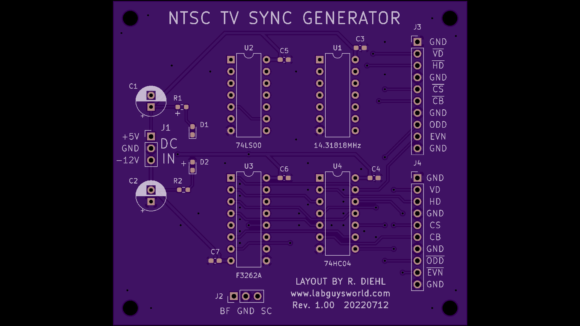
Creating the Printed Circuit Board My preferred desgn tools for this task are the Kicad suite of tools. The Kicad suite includes schematic capture, electrical rules checking, parts list, net list, and PCB tools. Draw the schematic, check it for errors, render the part list, render the net list, import the net list into the PCB tool, place the part footprints, define the outline of the board and then route and pour the copper layers. In most cases, the next step is to export the Gerber (layer) files. These are plain ASCII text files that define where to drill the holes, how big to make the holes, define the copper traces for each layer, define the solder mask for the top and bottom layers, and finally the top and bottom silk screen layers whcih contain the necessary identifying text. Some vendors, like the one I used, are able to accept the actual Kicad PCB project file directly. Otherwise, we send Gerber files to our favorite fabrication vendor. In this hobby, during schematic drafting, a lot of time is consumed by creating the rare part symbols in the library. Once these are completed, the schematic drafting is relatively easy. Kicad comes complete with a huge library of standard and common components. But, for the eclectic designer, a custom library is a must. Labguy probably has the most esoteric library of Kicad schematic parts of anyone. Image dissector tubes, Iconoscopes, CRTs, deflection yokes, etc. Click this logo to visit the Kicad site Kicad is free. We are currently using version 5.1.7 here at labguy's World. We plan to upgrade to version 6 in the near future. I recommend you start in version 6 if you are new to these tools. It is realtively easy to use. Though, if you are migrating from more advanced tools like PADs, Altium or or other high end EDA tools, it will be challenging to think "down" to this tool. If you are like me and didn't use 99% of the features in the expensive software, then Kicad is probably just the ticket for you too. For a free software suite, it works surprisingly well and is worth the investment of your time and effort to learn it. To get my board fabricated, I sent the project files to [OSH PARK]. As of 20120721, the cost of three boards was $41.25(US). Total time to delivery about 12 days. You can get your board from OSH Park in any color you like as long as it is purple. 
Click the pic for my email address. Charlie Anderson, Labguy and Fred Pfost [HOME] [ELECTRONICS PROJECTS] |