|
LabGuy's World: NBTV - 10-4 Eleanor! RGBY Color Video Signal Generator Project
[PREVIOUS PAGE] [HOME] [ELECTRONICS PROJECTS] [NEXT PAGE] [1. INTRODUCTION] [3. SOFTWARE] [4. IMAGES] [5. CONCLUSION] 2. HARDWARE 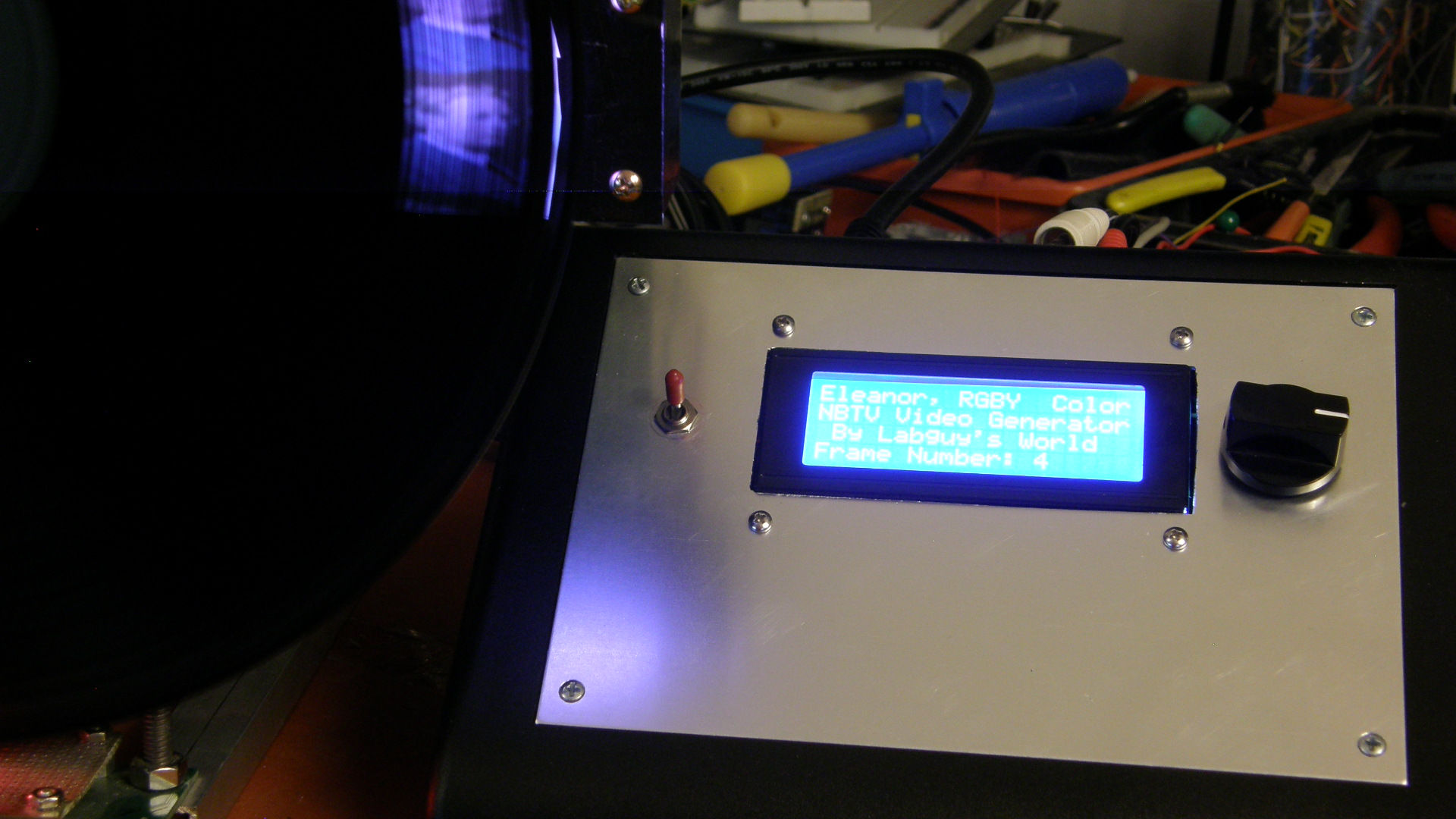


The 10-4 Eleanor - Hardware Physical Description The hardware of the 10-4 Eleanor consists of an NBTV video signal generating board and a simple Arduino microcontroller human interface. The front panel contains the DC power ON/OFF switch, a 20 character by 4 line LCD display and a rotary encoder / push button contol. The rotary control allows selection of one of 256 stored still images. The back panel supports the power supply input and the various video and sync output jacks. The electronics are housed in a plastic project box, with an aluminum sloped front panel, that measures 9 inches (23cm) wide by 7 inches (17cm) by 3 inches (7cm) thick. The power supply is an external brick style unit purchased on Ebay for about $30. It is an analog type vs the switching type. Either type will work. You may try to find this exact unit or use any adapter that is equivelant. This is not critical as long as the supply provides clean DC voltages at the required power levels. This particular power supply provides +5VDC at up to 1 amp and ±12VDC at up to 300mA each. The Eleanor uses nowhere near this much power. I made one modification. I added a power switch on the AC mains side of the transformer. There are enough vampire power supplies in the world already. 

The 10-4 Eleanor - Block Diagram and Internal Wiring Harness The video board contains three parallel video frame buffers, red, green and blue, each one containing 256 parallel NBTV images, of 2048 pixels each, stored in three half megabyte EEPROM memory chips. The NBTV frame format is described in greater detail on the [IMAGES] page. Timing drive pulses for the memories and video sync are generated by a very simple crystal controlled state machine based on another half megabyte EEPROM memory chip. How the timing and video memory chips are programmed is described in greater detail on the [SOFTWARE] page. Outputs are available as 75Ω terminated red, green and blue 1Vpp signals without sync and one simultaneous monochrome Composite Video Blanking and Sync (CVBS) signal, also when terminated into 75Ω. For color operation, the CVBS serves as the separate sync for the RGB signals. The only external control required by the video signal generator board, driven from the Arduino controller, is a single 8 bit output port on the I2C bus. This port selects which frame of stored video is presented on the output. The Arduino controller is interfaced with the rotary encoder / pushbutton control, the 4 line by 20 character LCD display and the control port on the video board. The latter two connected via the standard I2C bus. 


The 10-4 Eleanor Video Circuit Schematic Diagrams and Component Placement In the first schematic diagram we see three major sub sections of the 10-4 Eleanor circuit. Upper left is the master clock 4.096MHz crystal oscillator, 19 bit binary counter (3x 74HC590), the half megabyte timing memory chip (Silicon Technolgy part# 29F040) and an 8 bit deglitching latch (74HC574). These form the basic master timing generator also known as a state machine. In the upper right, is the I2C (eye squared see) parallel port (PCF8574N) driven by serial data from the Arduino Mega computer controller. It's function is to select one of two hundred fifty six images stored in the RGB video frame buffers covered on the next schematic page. The I2C port is followed by the frame sync latch (74HC574) that makes for clean switching when we change frame numbers. In the lower right is the luma and matrix circuit and the sync and blanking summer circuits that create the CVBS (Composite Video, Blanking & Sync) output signal. Across the bottom are the various power distribution details for the system and the opamp chips. The DC power pins on all chips are bypassed to ground with their own individual 100nF (.1µF) ceramic capacitors. The state machine circuit is extremely simple. A master clock oscillator, running at 4.096MHz, drives a simple 19 bit binary counter consisting of three 74HC590 eight bit binary counters in cascade. The outputs of these counters constitute the address locations in the flash memory chips. The timing patterns for clocking the rest of the system are stored in the memory chip and sequentially clocked out for the duration of one frame of video. Because the outputs of the memory chip are permanently enabled, it is possible for them to momentarily output random data, "glitches", as they settle to the next data location. So, to prevent the glitches from causing random misoperation of downstream devices, the glitches are removed by reclocking the signals with the external eight bit latch, U3, another 74HC574. The terminal count of the state machine is 327,680. At 4.096MHz, this adds up to 80mS or one frame time for video. At address 327,679 a zero is stored in the D0 bit postion. In all other locations for bit D0, there are ones. This is the pulse that resets the counters and starts the cycle all over again. The pulse is called statem maachine reset not and is symbolized as SM_RST. 
The 10-4 Eleanor State Machine Timing Diagram There are four primary timing pusles generated from the state machine. They are Pixel Clock (PXL_CLK) in bit position #1, Frame Reset Not (FRM_RST) in bit position #2, Composite Sync (COMP_SYNC) in bit position #3 and Composite Blanking (COMP_BLNK) in bit position #4. PXL_CLK drives the address counters for the video frame memories and the frame memory deglitching latches. FRM_RST resets the frame memory address counters at the end of each frame. COMP_BLNK cuts off the D/A outputs and clamps the luma signal to zero volts during the line sync intervals so that the COMP_SYNC can be added (algebraic subtraction) from the luma signal to create the composite video output. Essentially, sync is negative point 3 volts, referenced to zero volts DC and the analog video signal is up to point plus seven volts above zero volts DC. Looking at the System Control Ports, U14 and U15 in the upper right. U14 is a serial to parallel that works on the I2C bus. It receives the desired frame number from the Arduino processor and passes it to the 74HC574 eight bit parallel latch U15. This latch is clocked with the FRM_RST pulse. This assures that the frame changes during the blanking interval between video frames preventing the momentary display part of the last frame and part of the next frame. Frame changes will be seamless. The outputs of the I2C port are pulled up, not down as shown in the schematic. These ouptuts are of the open drain type and require pullup resisors in order to work. I was using the pull down resistors prior to the installation of the Arduino to guarantee that the frame buffer started with the first stored picture in location zero and not empty location 255. Lastly, let's examine the Composite Video, Blanking and Sync Matrix Amplifier. Analog RGB video, at a level of 2 volts each, is fed to a simple resistor matrix which adds them together in the proper proportions to create the lumanance signal called Y. The proportions are: 30% red plus 59% green plus 11% blue. The resistors, R6, RV5, RV6 and RV4 perform this addition and additionally divide the signal by 2. R6 (1.69K), RV5 (3.333K) and RV6 (9.09K) when connected in parallel add up to 1K and they are in series with RV4 which is also 1K. This 6dB voltage loss is made up by the following opamp running with a gain of 2, restoring the video level back to nearly one volt when RV4 is approximately centered. Actually the analog luma is set 0.7 volts. The output of the pot RV4 is passed through a series resistor R7, 499 ohms, so that the FET Q1 can clamp the line to zero volts during blanking for the addition of the sync pulse. The sync pulse level is set to -0.3 volts on the output by way of RV7, the sync level set pot. Alignment of the CVBS output is simple. Select frame zero, horizontal color bars and view the video signals on an oscilloscope terminated in 75 ohms on each channel. Adjust the D/A converters to output 1 volt video into the 75 ohm load. Next, set RV4 to the top of its range, and adjust RV5 and RV6 for the most even steps of grey on the CVBS output. Then set RV4 to give a peak white setting of +0.7 volts and set RV7 to give a sync tip level of -0.3 volts. The CVBS signal is now 1 volt peak to peak with blanking set to a level of zero volts DC. Easy peasy! Looking at the second page of the schematic, it couldn't get much simpler. Upper left are the two binary counters (74HC590, U16 & U18) that run the continuous 11 bit video address for counting pixels out of the three frame memories (U4, U10 and U19). On the upper left of each memory chip, you will see the eight frame select bits forming the upper byte of the memory addresss. The data outputs of the memory chips are coupled to the deglitching latches (74HC574, U5, U11 and U20). Note that all three of these memory busses have 4.7K pull down resistors attached. During video blanking, the outputs of the memory chips are disabled and placed in high Z mode. The resistors then present a binary zero to the inputs of the ddeglitching latches. This couples through to the three A/D converter chips (AD7533, U6, U12 and U21) forcing them to zero volts on their outputs during video blanking. That's the theory anyway. For whatever reason, blanking had to be reinserted in the Luma circuit to make sync addition work properly. No biggy. The putputs of the A/D converters, for whatever reason, go from zero volts to MINUS one volt! I could find no version of the reference circuits that produced a positive going output voltage in the data sheets or in the application notes for the AD7533 chips. Oh, well. So, my solution was to follow the D/A buffer opamps with a second set of opamps that inverted the video and amplified it by a gain of two. The gain of two is to compensate for the 2:1 voltage drop of the properly terminated 75 video line drive outputs. This is normal in ALL properly designed video systems. This completes the electronic circuits description for the 10-4 Eleanor video board. All of the files used in this project are available for download as a zip file on the [CONCLUSION] page of this article. [PREVIOUS PAGE] [HOME] [ELECTRONICS PROJECTS] [NEXT PAGE] [1. INTRODUCTION] [3. SOFTWARE] [4. IMAGES] [5. CONCLUSION] |